FR4 HASL Lead-Free Immersion Gold 6-Layer Double Side PCB Assembly
Double Side PCB Assembly Introduction
Double sided PCB is very similar to single sided PCBs, It has two sided traces with a top and bottom layer.
These boards can mount conductive copper and components on both sides of the circuit board, which allows the traces to cross over each other. This results in a higher density of circuits without the need of point-to-point soldering.
As these types of circuit boards are more complex than single sided PCBs, it can be more difficult to produce.
However, the benefits of using double sided PCBs far outweigh the cons.
PCB CAPABILITIES
| FACTORY CAPABILITIES |
| No. | Items | 2019 | 2020 |
| 1 | HDI Capabilities | HDI ELIC (4+2+4) | HDI ELIC(5+2+5) |
| 2 | Max layer count | 32L | 36L |
| 3 | Board Thickness | Core thickness 0.05mm-1.5mm ,Fineshed board thickness 0.3-3.5mm | Core thickness 0.05mm-1.5mm ,Fineshed board thickness 0.3-3.5mm |
| 4 | Min.Hole Size | Laser 0.075mm | Laser 0.05mm |
| Mechnical 0.15mm | Mechnical 0.15mm |
| 5 | Min Line Width/Space | 0.035mm/0.035mm | 0.030mm/0.030mm |
| 6 | Copper Thickness | 1/3oz-4oz | 1/3oz-6oz |
| 7 | Size Max Panel size | 700x610mm | 700x610mm |
| 8 | Registration Accuracy | +/-0.05mm | +/-0.05mm |
| 9 | Routing Accuracy | +/-0.075mm | +/-0.05mm |
| 10 | Min.BGA PAD | 0.15mm | 0.125mm |
| 11 | Max Aspect Ratio | 10:1 | 10:1 |
| 12 | Bow and Twist | 0.50% | 0.50% |
| 13 | Impedance Control Tolerance | +/-8% | +/-5% |
| 14 | Daily Output | 3,000m2 (Max capacity of equipment) | 4,000m2 (Max capacity of equipment) |
| 15 | Surface Finishing | ENEPING /ENIG /HASL /FINGER GOLD/IMMERSION TIN/SELECTIVE THICK GOLD |
| 16 | Raw Material | FR-4/Normal Tg/High Tg/Low Dk/HF FR4/PTEE/PI |
PCBA CAPABILITIES
| PCBA Capability |
| Material type | PCB | Components |
| Item | Dimension (Length, width,height. mm) | Material | Surface finish | Chip&IC | BGA Pitch | QFP Pitch |
| Min | 50*40*0.38 | FR-4,CEM-1,CEM-3,Aluminium-based board,Rogers,ceramic plate,FPC | HASL, OSP, Immersion gold, Flash Gold Finger | 1005 | 0.3mm | 0.3mm |
| Max | 600*400*4.2 | | |
Our SMT capabilities:
SMT Assembly: SMT provides a flexible high technology.
These solutions include:
7 high-speed placement machines,
7 automatic printers with fiducial alignment,
2 X-ray machines,
BGA maintenance machines,
ICT test machines
Our DIP function:
A-8 semi-assembly production line with four wave soldering machines
1 U-shaped automatic assembly line for box-type building products with test stations
High temperature / low temperature aging test furnace B-4 for products required for aging test
With time control and temperature control
All products are 100% inspected and tested during the DIP process
Haina lean Electronics Co.,Ltd is a competitive China customize pcba for medical breathing machine OEM manufacturer, supplier and vendor, you can get quick turn customize pcba for medical breathing machine production prototypes and samples from our factory.
Hot Tags: customize pcba for medical breathing machine, China, supplier, manufacturer, factory, OEM manufacturer, vendor, samples, production, prototypes, quick turn
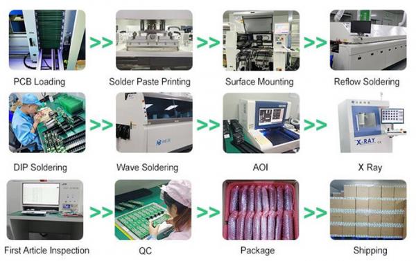
Double Side PCB Assembly Process
1.Solder Paste stenciling---2.Surface Mount Technology (Pick and Place)---3.Reflow Soldering---4.Inspection and Quality Control---5.Through-Hole Component Insertion (DIP Process)---6.Final Inspection and Functional Test
Our advantage
1.Service value
Independent quotation system to quickly serve the market
2.PCB manufacturing
High-tech PCB and PCB assembly production line
3.Material purchasing
A team of experienced electronic component procurement engineers
4.SMT post soldering
Dust-free workshop, high-end SMT patch processing
Similar products


Double Side PCB Assembly Delivery Time
| Product Type | Qty | Normal lead time | Quick-turn lead time |
| SMT+DIP | 1-50 | 1WD-2WD | 8H |
| SMT+DIP | 51-200 | 2WD-3WD | 1.5WD |
| SMT+DIP | 201-2000 | 3WD-4WD | 2WD |
| SMT+DIP | ≥2001 | 4WD-5WD | 3WD |
| PCBA(2-4Layer) | 1-50 | 2.5WD-3.5WD | 1WD |
| PCBA(2-4Layer) | 51-2000 | 5WD-6WD | 2.5WD |
| PCBA(2-4Layer) | ≥2001 | ≥7WD | 5WD |
| PCBA(6-10Layer) | 1-50 | 3WD-4WD | 2.5WD |
| PCBA(6-10Layer) | 51-2000 | 7WD-8WD | 6WD |
| PCBA(10-HDILayer) | 1-50 | 7WD-9WD | 5WD |
| PCBA(10-HDILayer) | 51-2000 | 9WD-11WD | 7WD |
Why choose us?
1. We are the manufacturer/ factory; Welcome to visit us one day.
2. We have good quality control systems, including AOI, ISO 9001 etc. ;
3. All the material we use have the RoHS identify;
4. All the components we use are the New & Original;
5. One-stop service can be provided from PCB design, 1-36 layers PCB manufacturing, components sourcing, PCB Assembly, to Fully Product Assembly.
Double Side PCB Assembly Application Field
Our products are widely used in
1.communication equipment,
2.industrial control,
3.consumer electronics,
4.medical equipment,
5.aerospace,
6.light-emitting diode lighting,
7.automotive electronics etc

Workshop


Common packaging
1.PCB: Vacuum packaging with carton box
2.PCBA: ESD packaging with carton box

Company Information
Beijing Haina lean Electronics Co.,Ltd is one of the most professional PCB manufacture in Beijing,China. With more then 10 years of development, Haina Lean Electronics turns into a first class manufacture of HDI PCB ,with production capability 4000 square meters.
Our factory is providing high quality bare PCB, PCB layout design service and PCB assembly service,including components sourcing, function test,conformal coating and complete assembly for clients all.

Product Tags:

|
|
Immersion Gold 6 Layer Double Side PCB Assembly , FR4 HASL Lead Free PCB Assembly Images
|